")
Do you yearn for an immediate increase in reliability of your engineering processes? Do you need that missing confidence that your electronics are not prone to failure during application?
If yes, your solution lies in Environmental Stress Screening (ESS), which is a set of intense screening processes designed for identifying potential failures in a product, either workmanship errors, design flaws or materials defects.
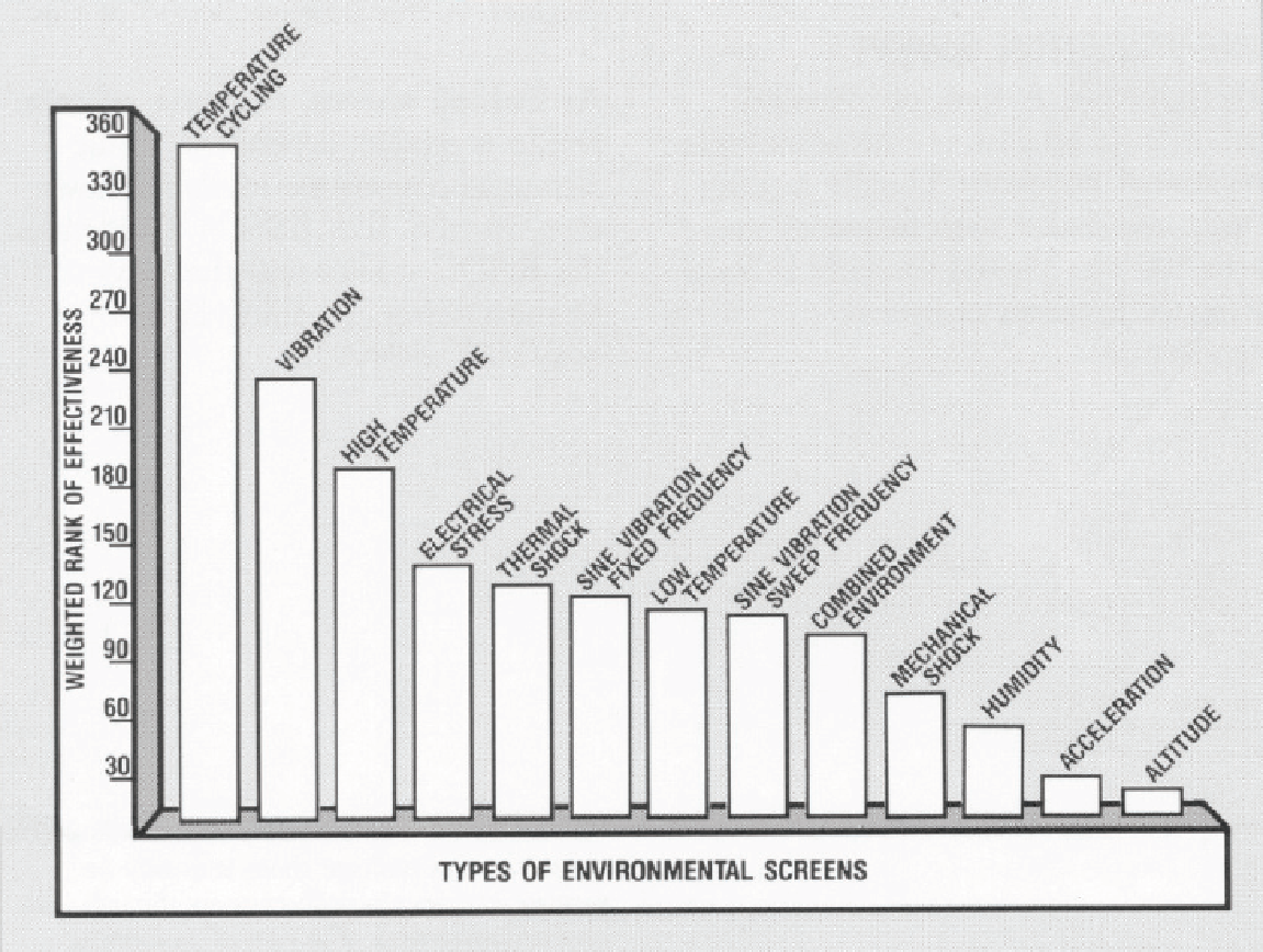
Fig 1: Types of Environmental Screening Tests (The Environmental Stress Screening Handbook)
MADES performs ESS processes to increase electronic reliability and minimize costs to our customer and the end user.
But ESS has a number of challenges.
Process and Other Challenges
Every electronic product has its unique potential flaws. ESS stress will consequently affect every item differently. Each product must have its own ESS process set-up. That is why ESS is identified as a product-specific process.
In implementing ESS, the stress processes applied to the electronic product are not exactly what real-life use offers. Simultaneous or sequential application of vibration and temperature cycling, as is the case in most products, may not provide the truest picture of real-life scenarios.
The need to monitor the electronic equipment during the screening process can be a challenge. Extreme conditions can cause unique failures that can only be detected by a keen eye.
On top of that, ESS is characterized by a high temperature range, but within the limitations of the product. A minimum temperature range of 100̊ C is usually recommended. The temperature alteration rate can be set at 10 to 15ºC per minute although it has to be jointly designed with the actual high and low temperature values and the number of cycles. and the temperature chamber must guarantee a uniform temperature distribution across the device under test.
ESS is in itself a potential cause for reversible damage to the electronic equipment. Ambient condition tests may never unearth such damages. Some of the field defects on electronic components could be from the ESS process. Designing the right ESS process has to take into consideration such potential latent damages occurred during the ESS process and undetected.
ESS Screening by MADES
You don’t have to endure these challenges, especially if you lack the capacity to conduct ESS. Professional testing services offered by MADES come packaged for the most reliable electronic product. We know that each electronic system and client are unique, so we design our testing strategies with that as the basis. Our complete series of electronic, functional and environmental computerized tests are designed to rate new designs and to guarantee consistent quality.
Environmental stress screening is one of the most popular electronic screening procedures, alongside functional tests and parametric electrical tests. At MADES, we offer the famed Highly Accelerated Life Testing (HALT) and Highly Accelerated Stress Screening (HASS), as well as other tests such as Vibe and Thermal.
HALT is a combination of modalities such as thermal shock, thermal cycling and vibration. You will find these in electronics, military, aerospace and other essential industries. HALT is an excellent method because it optimizes product reliability by stressing it beyond design specifications.
HALT helps determine operating limits, after which HASS testing can help identifying products that have higher warranty returns once there are alterations to the production process or product.
MADES Environmental Stress Screening Benefits
- We handle all sizes of projects, including high-volume ones.
- We are highly experienced in developing and improving ESS programs.
- With our specialized facilities and equipment, performing ESS with us is usually more efficient and economical.
- Our customers use our ESS services with immense success for all parties.


